6G Plastic Panels Developed by Finnish Scientists to Route Signals


Innovative Plastic Panels for 6G Signal Routing Unveiled by Researchers
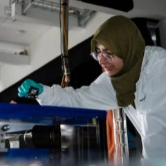
According to НВ — Техно: On June 8, a team of Finnish researchers introduced a breakthrough in wireless communication: 3D-printed metacrystalline panels made from ordinary plastic. These panels can be mounted on walls or furniture to reflect radio waves without requiring microchips or electricity. This development is particularly significant as future 6G networks aim to deliver data at speeds of terabits per second.
High-frequency 6G signals are prone to interference from obstacles like walls and crowds, making transmission challenging. The volumetric metacrystals designed by the Finnish team can handle multiple incoming signals or frequency bands simultaneously, a critical feature for ensuring reliable wireless connectivity.
Unlike earlier single-layer intelligent surfaces, these volumetric metacrystals can be engineered to independently manage several incoming signals or frequency bands.
Mahdi Asghari, one of the researchers
Producing a single metacrystalline panel costs just a few dozen euros, making them affordable for widespread use. The scientists are actively seeking partners to commercialize the project and are also developing new device configurations that can automatically adapt to environmental changes.
When a room is too dark, you can bring in more lamps-or use simple mirrors to direct the existing light. That's exactly what these metacrystals do, but with radio waves.
Mahdi Asghari, one of the researchers
In essence, the creation of metacrystalline panels opens up new possibilities for advancing 6G technology, enhancing communication quality and ensuring high data transfer speeds even in challenging conditions. This innovation could be a major step toward solving the limited bandwidth issues in wireless networks, paving the way for broader 6G adoption in everyday life.
Successful commercialization of these panels has the potential to transform wireless communication approaches, offering new opportunities for both users and businesses.
As advancements in communication technology continue to evolve, innovations in chip production are equally crucial. A recent article highlights how a novel nanostructure method is streamlining the manufacturing process for chips, which are essential components in modern electronics. To explore how these developments can impact the future of technology, read more about this efficient approach to chip manufacturing.
Read also