Chip Manufacturing Gets a Boost: Novel Nanostructure Approach Streamlines Production

Breakthrough in Nanostructure Fabrication
According to НВ — Техно: On May 25 at 5:00 PM, details emerged about a new technique for creating nanostructures on insulating substrates. This method leverages an anisotropic crystal of alpha-molybdenum trioxide and an electron beam, dramatically simplifying semiconductor production. It enables the formation of chip topologies capable of transmitting both electronic and optical signals, which is expected to accelerate semiconductor manufacturing. This innovation addresses a key challenge in the industry, where integrating photonic components with traditional electronics has long been a bottleneck.
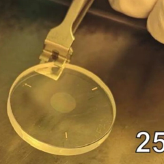
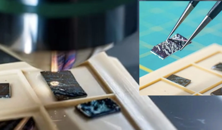
Conventional processes for building nanostructures on silicon dioxide are multi-step, costly, and rely on harsh chemicals. In contrast, the new approach involves depositing a layer of anisotropic alpha-molybdenum trioxide crystal on top of the silicon dioxide. Exposure to an electron beam triggers bond rearrangement, softening of the substrate, and directional stress, resulting in a well-ordered pattern of uniform folds on the surface.
Advantages of the New Method
These folds measure hundreds of nanometers in size and can refract and split light, making them suitable for use as optical gratings. The pattern's configuration can be tuned by adjusting the crystalline layer's thickness or the radiation intensity. The auxiliary molybdenum layer is easily removed after processing. This effect has also been confirmed on aluminum oxide and silicon nitride substrates.
This technique opens the door to creating complex optical structures in a single, straightforward step on standard materials. Researchers hope this discovery will significantly speed up semiconductor production and drive the rapid development of next-generation photonic and optoelectronic devices. The ability to integrate advanced light-based technologies into future microchips greatly simplifies the path to their realization.
This novel nanostructure approach could fundamentally transform the semiconductor industry by cutting both costs and production time for chip fabrication. Integrating light-based technologies into microchips may unlock new possibilities across computing, telecommunications, and medical devices, underscoring the importance of this research for the future of technology.
Read also