Room-Temperature Nanostructure Fabrication Method for Chips Unveiled

A Breakthrough in Nanostructure Engineering
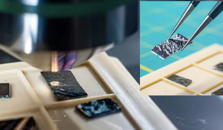
According to НВ — Техно: On May 25, 2026, at 5:00 PM, news.rice.edu reported a novel technique for creating nanostructures on chip materials-all at room temperature. This method employs an anisotropic crystal of alpha-molybdenum trioxide placed atop silicon dioxide. During fabrication, an electron beam irradiates the materials, generating folds measuring hundreds of nanometers in size.
To put this precision into perspective, these folds are thinner than a human hair. The pattern configuration can be adjusted by modifying the crystalline layer's thickness or the radiation intensity. Once the process is complete, the auxiliary molybdenum layer is easily removed, making nanostructure creation more convenient and efficient.
Implications for Semiconductor Technology
Research has also confirmed a similar effect on aluminum oxide and silicon nitride. This new technology opens fresh possibilities for semiconductor manufacturing, significantly speeding up production. The discovery is poised to have a major impact on the semiconductor industry, which constantly demands improvement and innovation.
“The new nanostructure fabrication method based on alpha-molybdenum trioxide could fundamentally change chip manufacturing approaches” – source: news.rice.edu
As competition in the semiconductor sector intensifies, such innovations become critical for maintaining rapid technological progress. This breakthrough also highlights the potential of materials science research, paving the way for new applications across various tech industries.
Read also